ADVANCED CMOS TECHNOLOGY 2023 (THE 5/3/2 NM NODES)
To accommodate the travel restrictions imposed by the COVID-19 pandemic
this class will be held online.

The course has been newly updated to include all of the latest developments in CMOS technology and is technically current.

| Course Date: |
October 6, 7, 8, 2021 (PDT) |
| |
|
| Course Length: |
Three Days |
| Tuition: |
$1,895 (USD) |
Course Description:
The central theme of this seminar is an in-depth presentation of the key 5/3 nm node technical issues for Logic and Memory, including detailed process flows for these technologies.
This course addresses the issues associated with Advanced CMOS manufacturing with technical depth and conceptual clarity, and presents leading-edge process solutions to the new and novel set of problems presented by 5 nm FinFET technology and previews the upcoming manufacturing issues of 3nm Nanosheets.
What's Included:
- Three days of instruction by industry experts with comprehensive, in-depth knowledge of the subject material
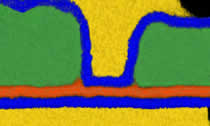
- A high quality set of full-color lecture notes, including SEM & TEM micrographs of real-world IC structures that illustrate key technical points
- A Diploma stating that you have successfully completed the seminar will be mailed to you at the end of the course
Course Topics:
 1. Process integration. The 5/3 nm technology nodes represent a landmark in semiconductor manufacturing and they employs transistors that are faster and smaller than anything previously fabricated. However, such performance comes at a significant increase in processing complexity and requires the solution of some very fundamental scaling and fabrication issues, as well as the introduction of radical, new approaches to semiconductor manufacturing. This section of the course highlights the key changes introduced at the 5/3nm nodes and describes the technical issues that had to be resolved in order to make these nodes a reality.
- The enduring myth of a technology node
- Market forces: the shift to mobile
- The Idsat equation
- Ion/Ioff curves, scaling methodology
- The Standard Cell Concept
- Buried Power Rails
2. Detailed 7nm Fabrication Sequence. The FinFET represents a radical departure in transistor architecture. It also presents dramatic performance increases as well as novel fabrication issues. The 5nm FinFET is the 5th generation of non-planar transistor and involves some radical changes in manufacturing methodology. The FinFET’s unusual structure makes its architecture difficult for even experienced processing engineers to understand. This section of the course drills down into the details of 5 nm FinFet structure and its fabrication, highlighting the novel manufacturing issues this new type of transistor presents. A detailed step-by-step 5 nm fabrication sequence is presented (Front-end and Backend) that employs colorful 3D graphics to clearly and effectively communicate the novel FinFET architecture at each step of the fabrication process. Attention to key manufacturing pitfalls and specialty material requirements are pointed out at each phase of the manufacturing process, as well as the chemistries used at each operation.
- Self-Aligned Quadruple Patterning (SAQP)
- Germanium PMOS fin fabrication
- Multiple Vt Hi-/Metal Gate integration strategies
- Cobalt Contacts & Cobalt metallization
- Contact over Active Gate methodology
- Tone Reversal Metallization methodology
- Air-gap dielectrics
3. Nanosheet Fabrication. Waiting in the wings is the 3nm Nanosheet. The advent of this new and radically different 3D transistor features gate-all-around control of short channel effects and a high level of scalability. A detailed process flow of a 3nm Nanosheet fabrication process will be presented that is beautifully illustrated with colorful 3D graphics and which is technically accurate.
- A detailed 3nm Nanosheet fabrication process flow
- Key fabrication details and manufacturing problems
- Nanosheet SCE control and scaling
- Resolving Nanosheet capacitive coupling issues
- Vertical versus Horizontal Nanosheet architecture: advantages and disadvantage
 4. DRAM Memory. DRAM memory has evolved through many generations and multiple incarnations. Despite claims that DRAM memory is nearing its scaling limit, new technological developments keep pushing the scaling envelope to extremes. This part of the course examines the evolution of DRAM memory and presents a detailed DRAM process fabrication flow.
- DRAM memory function and nomenclature
- DRAM scaling limits
- A DRAM process flow
- The Saddle Fin Transistor
- Storage Node Fabrication
5. 3D NAND Flash Memory. The advent of 3D NAND Flash memory is a game changer. 3D NAND Flash not only dramatically increases non-volatile memory capacity, it will also add at least three generations to the life of this memory technology. However, the structure and fabrication of this type of memory is radically different, even alien, to any traditional semiconductor fabrication methodology. This section of the course presents a step-by-step visual description of the unusual manufacturing methodology used to create 3D Flash memory, focusing on key problem areas and equipment opportunities. The fabrication methodology is presented as a series of short videos that clearly demonstrate the fabrication operations at each step of the process flow.
- staircase fabrication methodology
- the role of ALD in 3D Flash fabrication
- controlling CDs in tall, vertical structures
- detailed sequential video presentation of Samsung 3D NAND Flash
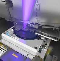 6. Advanced Lithography. Lithography is the “heartbeat” of semiconductor manufacturing and EUV is now entering production. Without EUV lithography continued scaling would difficult, if not impossible. Recently there have been significant breakthroughs in Extreme Ultra Violet (EUV) lithography that has allowed it to enter mainstream manufacturing. This section of the course begins with a concise and technically correct introduction to the subject and then provides in-depth insights into the latest developments in photolithography. Special attention is paid to EUV lithography, its capability, characteristics and the recent advancements in this field.
- Physical Limits of Lithography Tools
- Immersion Lithography – principles and practice
- Double and Quadruple patterning
- EUV Lithography: status, problems and solutions
- EUV in high-volume manufacturing
- High Numerical aperture EUV
 7. Emerging Memory Technologies.
There are at least three novel memory technologies entering production. Unlike traditional memory technologies that depend on electronic charge to store data, these memory technologies rely on resistance changes. Each type of memory has its own respective advantages and disadvantages and each one has the potential to play an important role in the evolution of electronic memory.
7. Emerging Memory Technologies.
There are at least three novel memory technologies entering production. Unlike traditional memory technologies that depend on electronic charge to store data, these memory technologies rely on resistance changes. Each type of memory has its own respective advantages and disadvantages and each one has the potential to play an important role in the evolution of electronic memory.
This section of the course will examine each type memory, discuss how it works, and what its relative advantages are in comparison with other new memory types.
- Phase Change Memory (PCRAM), Cross-point memory; separating the hype from the reality
- Resistive RAM (ReRAM) – a novel approach that comes in two variations
- Spin Torque Transfer RAM (STT-RAM) – the brightest prospect?
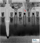 8. Survey of leading edge devices. This part of the course presents a visual feast of TEMs and SEMs of real-world, leading edge devices for Logic, DRAM and Flash memory. The key architectural characteristics for a wide range of key devices will be presented and the engineering trade-offs and compromises that resulted in their specific architectures will be discussed. The Fellow Emeritus representative of the world’s leading chip reverse engineering firm will present the section of the course.
- How to interpret Scanning and Transmission Electron microscopy images
- A visual evolution of replacement gate metallization
- DRAM structural analysis
- 3D FLASH structural analysis
- Currently available 7/5nm Logic offerings from various manufacturers
 9. 3D Packaging Versus 3D Monolithic Fabrication. Unlike all other forms of advanced packaging that communicate by routing signals off the chip, 3D packaging permits multiple chips to be stacked on top of each other, and to communicate with each other using Thru-Silicon Vias (TSVs), as if they were all one unified microchip. An alternate is the 3D Monolithic approach, in which a second device layer is fabricated on a pre-existing device layer and electrically connected together employing standard nano-dimensional interconnects. Both approaches have advantages and disadvantages and promise to create a revolution in the functionality, performance and the design of electronic systems.
This part of the course identifies the underlying technological forces that have driven the development of Monolithic fabrication and 3D packaging, how they are designed and manufactured, and what the key technical hurdles are to the widespread adoption of these revolutionary technologies.
- TSV technology: design, processing and production
- Interposers: the shortcut to 3D packaging
- The 3D Monolithic fabrication process
- Annealing 3D Monolithic structures
- Foveros and EMIB technology
 10. The Way forward: a CMOS technology forecast. Ultimately, all good things must come to an end, and the end of FinFET technology is within sight. No discussion of advanced CMOS technology is complete without a peek into the future, and this final section of the course looks ahead to the 3/2/1 nm CMOS nodes and forecasts the evolution of CMOS device technology for Logic, DRAM and Flash memory.
- The Upcoming changes to FinFET architecture and fabrication
- New metallization schemes
- The next ten years
- Is Moore’s law finally coming to an end?