10/7 NM FinFet Fabrication


Course Description:
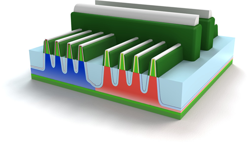
FinFet manufacturing is novel, non-intuitive, and difficult to decode simply
from reading research papers. It presents a range of non-traditional fabrication
methodologies that even veteran device engineers find disorienting.
This
one-day course demystifies the science of FinFet fabrication by presenting a
technically accurate explanation of the processing operations required to
manufacture a 10/7nm FinFET. The entire fabrication process is presented in
step-by-step detail using high-quality 3D illustrations and TEMs of real-world
FinFet devices. The key manufacturing issues associated with each step of the
process are discussed, as well as the central differences between FinFet and
planar manufacturing.
The course is presented in a highly visual format with
detailed high-quality color illustrations of every aspect of the FinFet
fabrication process. All aspects of the 10/7nm fabrication process are presented
in depth.
Download this seminar brochure as a .pdf file

Date: To Be Announced
Location: To Be Announced
Tuition: $795
 What’s Included:
- A full day of instruction by an industry expert with an in-depth understanding
of the course material.
- A high quality set of course notes that are in full color.
- Continental breakfast, hot buffet lunch and snacks at the morning and afternoon
breaks.
This course is intended for:
- Device, Test and Process engineers
- Failure analysis engineers
- Equipment engineers
- Designers
- Fab interface engineers
- Patent Attorneys
- Managers and other personnel who desire a deeper understanding 22nm FinFet processing
Course Topics:
-
Introduction to the basic processing modules
- Shallow Trench Isolation & Well formation - the new reality
- Fin fabrication: Self-Aligned Double Patterning (SADP) versus Self-Aligned Quadruple pattering (SAQP)
- FinFET gate-last Hi-k/Metal gate integration methodology
- Multiple Vt Work Function metals
- Replacement gate metallurgy & integration strategies for FinFETs
- Strained silicon using SiP and SiGe replacement Source/Drains
- Titanium “Salicidation” integration methodology
- Key FinFET fabrication issues and their solutions
- Line-Etch-Line-Etch (LELE) Double patterning
- SADP for Gate electrode fabrication & Cobalt contact implementation
- Copper metallization and Low-K dielectric fabrication including “Air Gap” dielectrics
- Back-end capacitor formation details
The Future:
-
How will the 7nm FinFET differ from the 10nm FinFET?
- What options are available for the 5nm node?
- Nanowires - the sub-7nm node option
The Instructor:
Jerry Healey
Jerry Healey has been a technical professional in the semiconductor industry for over 25 years, 8 years of which were spent as a Device Engineer at Motorola Semiconductor. He was formerly an instructor for UC Berkeley Extension (College of Engineering), and more recently was employed as a Process Integration Engineer at the Advanced Technology Development Facility, where he worked on advanced technology node development.
He is a renowned lecturer in the field of silicon processing, and his areas of expertise include process integration, technology transfer of new processes from R&D into manufacturing, 3D Packaging and FinFET fabrication. His audiences remember him for the breadth of his knowledge regarding semiconductor manufacturing, his engaging lecture style, and the insightful 3D color graphics he uses to illustrate his lectures.
An award winning public speaker, Mr. Healey has taught numerous courses to thousands of practicing engineers and scientists over the past 15 years. He has also authored numerous papers in the field of silicon processing, and is currently the president of Threshold Systems, a firm that provides consulting services and technical training seminars to the semiconductor industry.
Download Resume
Testimonials
“The level of reverse engineering in this course is incredible and the instructor’s knowledge of silicon processing is excellent. I am gong to send all of my direct reports to this course.” – S. Richardson
“The level of detail in this course is very impressive and the 3D graphics were most enlightening.” - Jin Yung