Lithography for Nano-Technology CMOS ICs

This one-day course describes the state-of-the-art and latest advances in lithography for today’s most advanced CMOS nanotechnology ICs.
Course Description:
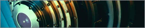
This course provides a broad, deep treatment of lithography, the key driving technology in CMOS IC fabrication. It covers all critical lithographic technology elements, from basic concepts to leading-edge technology and applications issues for today’s most advanced CMOS nanotechnology ICs. It then describes the variations in lithographic technology and circuit layout design techniques that are required to optimize performance and control variation in different IC applications for logic and memory. The material is presented using intuitive visual illustrations linked to relevant physics equations, supported by 2D & 3D graphics and numerous SEM and TEM photographs of real-world, leading-edge CMOS lithographic structures.
The course begins with a crisp overview of the lithography technology elements and basic concepts. It then describes in detail all leading-edge advances and issues in photoresist, masks, resolution enhancement techniques (RET), and exposure tools. It then presents an in-depth treatment of the latest advances in double and triple patterning technologies, computational lithography, and an extensive explanation of EUV (Extreme Ultra-Violet) technology, its challenges, manufacturing issues and current status.
Download this seminar brochure as a .pdf file

Date: To Be Announced
Location: To Be Announced
Tuition: $795
What’s Included:
- A full day of instruction by an industry expert with an in-depth understanding of the course material.
- A high quality set of course notes that are in full color.
- Continental breakfast, hot buffet lunch and snacks at the morning and afternoon breaks.
Course Topics:
- Lithography for CMOS nanotechnology ICs – equipment & process
- Overview of lithographic technology elements & review of basic process and equipment concepts
- Scanner exposure technologies
- Deep UV chemically amplified resist technology and applications issues
- Resolution/throughput/CD control trade-offs, contrast, substrate reflectivity control, etch resistance, line edge roughness (LER), pattern collapse, process variation
- Sub-wavelength lithography with resolution enhancement techniques (RET)
- Sub-wavelength lithography gap & technology roadmap through 14/10/7nm
- Resolution Enhancement Technology: customized illumination, optical proximity correction (OPC) and sub-resolution assist features (SRAFs), phase shift masks, double exposure techniques, photoresist feature shrink techniques
- Immersion lithography technology – principles and
- Double and triple patterning technologies
- Computational lithography technology – how it extends 193nm optical lithography
- EUV – challenges, issues and current status: power source ratings, WPH manufacturability, EUV reticles and implementation schedule